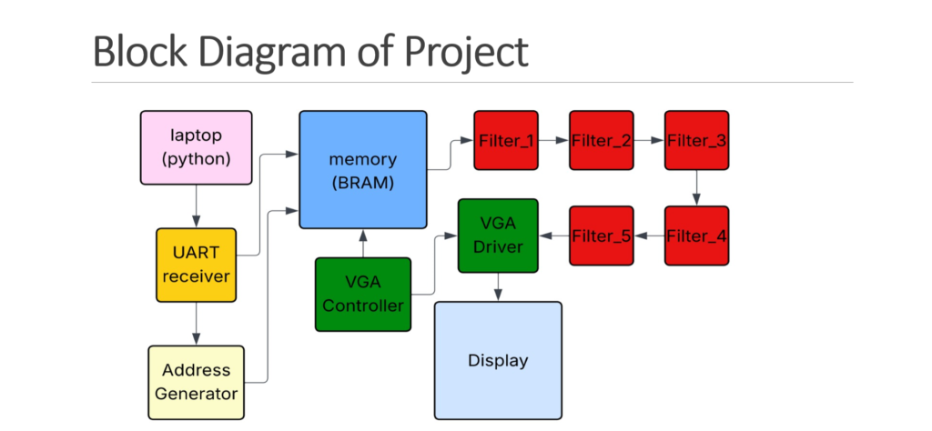
This project aims to develop a custom hardware-accelerated photo viewer and image processor that runs on an FPGA development board. It receives a digital image from a computer, stores it in the FPGA’s internal memory, applies selected image filters using hardware-based processing, and outputs the final result to a VGA monitor.
Project Overview
The system takes a digital image from a computer, saves it in the FPGA’s internal memory, applies various filters, and sends the outcome to a VGA monitor.
Key Functionality
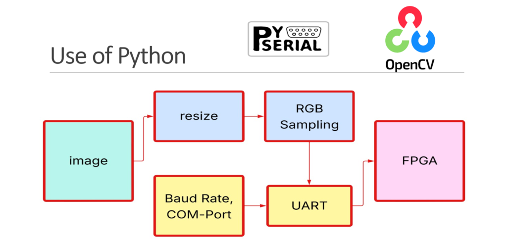
Image Input: A Python program on a PC transmits QVGA (320×240) image data (RGB444) through USB-to-UART (Universal Asynchronous Receiver-Transmitter).
On-Chip Storage: The FPGA employs a Dual-Port Block RAM (BRAM) for storing the entire image frame.
Display & Filtering: A custom VGA Controller retrieves the saved image and shows it on a monitor (640×480 @ 60 Hz), scaling the QVGA image to fit the screen.
Mode Control: A physical display switch changes the state of the FPGA: * Switch OFF: Receive Mode (the FPGA listens to UART and writes data to the memory). * Switch ON: Display Mode (the FPGA stops receiving data and continuously shows the stored image).
Filter Application: Various filters, including Convolution (like Blur), can be applied simultaneously using dedicated hardware logic controlled by slide switches.
Tools and Technologies
| Category | Component/ Language | Details |
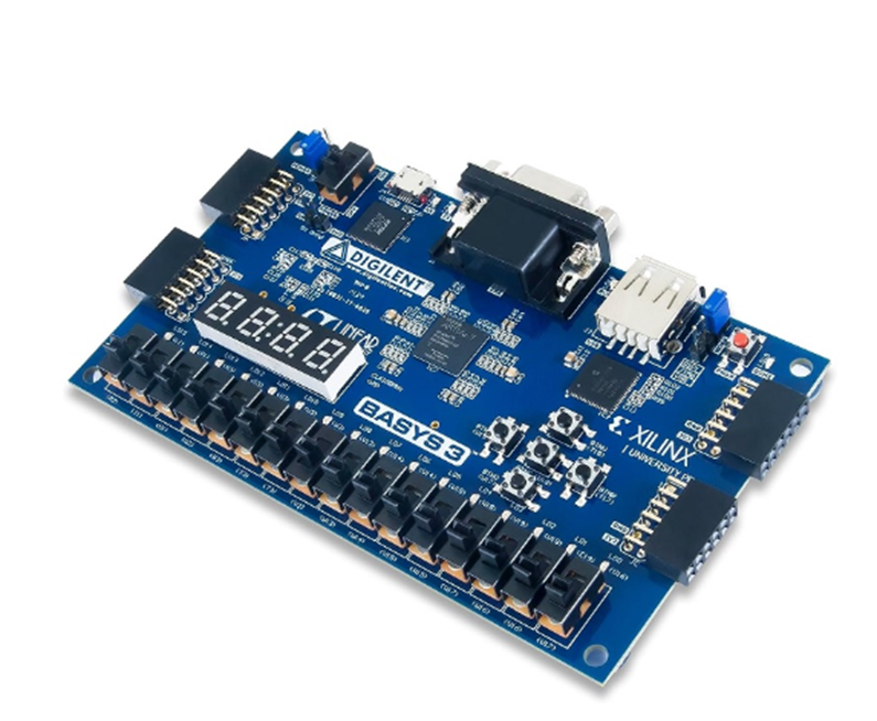
| Hardware | Basys 3 FPGA Board | Target board(Xilinx Artix-7, xc7a35t-1) |
| HDL | Verilog | Used for all Register-Transfer Level (RTL) design |
| Software | AMD Vivado Design Suite | For synthesis, implementation, and simulation |
| PC Scripts | Python (OpenCV, PySerial) | Used for image resizing, RGB sampling, and sending pixel data via UART |
| Protocols | UART & VGA | For data transmission and video display, respectively. |
RTL Design Modules
The core functions are built using several interconnected Verilog modules:
UART_Rx: This module receives serial data bytes from the computer.
Pixel_Compiler: It merges three consecutive 4-bit bytes (R, G, B) into a single 12-bit RGB444 pixel value, utilizing a Finite State Machine (FSM).
DualPort_RAM: Manages the on-chip BRAM for dual operations: writing (receive mode) and reading (display mode).
VGA_Controller: Generates timing signals (VSync, HSync, Pixel_Clock) necessary for the 640×480 @ 60 Hz display standard.

LineBuffer: Implements FIFO (First-In, First-Out) registers to temporarily store neighboring pixels (a 3×3 window) needed for convolution operations.
Convolution: Conducts matrix multiplication on the buffered pixel window to apply filters like blurring.
Top_Module: Instantiates and connects all the submodules, managing memory addresses and providing the final VGA output signals.
Equipments Used

Testing and Verification
The project includes steps for behavioral simulation and hardware testing:
Convolution Test: Behavioral simulations are run on grayscale images to confirm the functionality of the Convolution module before full integration.
Peripherals Test: Uses the built-in self-tests of the Basys 3 to ensure that the slide switches, UART data transmission, and VGA output are working correctly.
For further information visit(HackMD)
Members
Harshita Umashankar
Aditya Gaddam
Ashish Singh
Mentors
Kumar Ayush
Sanyam Gupta